From CMOS to ADAS: Gianluca Colli’s Interview About Imaging Sensor Innovations

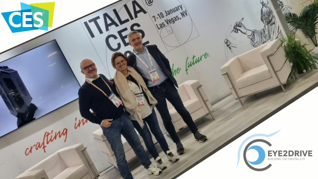
Eye2Drive is proud to welcome Gianluca Colli as our new Senior Advisor. Gianluca brings over 30 years of expertise in the semiconductor and imaging sensor industries, having held key roles at STM, National Semiconductor, Texas Instruments, and ONSEMI. His career is marked by significant leadership positions, including managing divisions with substantial annual revenues.
In this interview, Gianluca discusses the significant technological advancements in imaging sensors, particularly in CMOS Image Sensor technology. He highlights the shift driven by mobile applications and the subsequent impact of ADAS, autonomous driving, and industrial machine vision. These changes have led to a surge in market demand and innovations such as HDR capabilities, global shutter technology, and stack wafer processes.
Looking ahead, Gianluca foresees continued evolution in imaging sensor technology for autonomous vehicles, emphasizing the need for higher resolution, improved HDR performance, and triple-stack wafer technology. He notes the challenges of integrating various sensors and the critical role of AI in data analysis, advising automotive executives to prioritize quality and performance while reducing overall system costs.
Gianluca underscores the strategic importance of advanced imaging devices in autonomous systems, emphasizing their role in providing precise data for navigation and decision-making. He predicts substantial growth in the semiconductor and imaging sensor industries, driven by AI advancements, electrification, and new process technologies.
Expressing confidence in Eye2Drive‘s technology, Gianluca highlights its potential across various applications, from transportation to smart homes. He praises the company’s innovative approach to HDR performance in global shutter CMOS sensors and anticipates further developments.
Eye2Drive is excited to leverage Gianluca Colli’s extensive knowledge and experience to advance our mission in the dynamic world of imaging sensor technology.
Hi Gianluca, thank you for being available for an interview with Eye2Drive. Please briefly explain your professional background and journey in the semiconductor and imaging sensor industries.
First of all, thank you for having me here. Let’s start just with a few notes about my professional experience. I have a degree in Electronics Engineering from the University of Pavia with a specialization in Microelectronics, which means Analog circuit design in my specific case. After a few years as a researcher at my University, I joined STM in Agrate Brianza in CR&D. In 1996, I moved as Sr. Analog Designer to the STM San Jose Design Center, working on Data Storage custom IC design. In 2001, I left STM to join National Semiconductor, where I had several technical management roles, starting with design and expanding to test development, product engineering, and management. In 2006, I had my first full P&L role in designing, developing, and selling power management devices for Mobile applications. In 2011, I joined Texas Instruments through their National acquisition, where I held full P&L responsibility again as GM of one of their power management businesses. In 2015, I left and joined ONSEMI as VP and GM of the Mobile and Consumer Image Sensor Division. After exiting the mobile business, I also took over the image-sensing industry. In my role, I was responsible for long-term division Strategy, roadmaps, new product development, marketing, customer interaction, and overall P&L for the division, about $450M in revenue annually. Finally, in 2022, I decided to retire after 30 years in the Semiconductor business and enjoy my hobbies and family. I still live in Silicon Valley, California.
What key technological advancements in imaging sensors did you witness during your career?
I have been involved in the CMOS Image Sensor business for the last ten years, and I have to say, a lot has happened since then. Ten years ago, image sensor technology was still heavily driven by mobile phones and, generally, by applications where image sensors were used in devices for taking pictures and videos such as Security Camera, Portable Cameras (GoPro), and Computing, both integrated or stand-alone. Other applications driven by Machine Vision requirements were still addressed mainly by CCD and were niche markets. Since 2015, we saw two significant technology trends taking over in the Automotive and Industrial markets: ADAS and then Autonomous driving and Machine Vision applications such as Robotics, Scanning (2D and 3D), High-End Security systems (face recognition, object recognition, AI), AGV for warehouse and Agriculture, manufacturing inspection and so on. All these new applications have driven a 10x market growth in units sold (at least) and have pushed for a new set of requirements for image sensors because now data has to be handled by machines and not any more human eyes. HDR requirements have become extremely important, driving new pixel architecture, capability to “see” beyond the visible range (IR and beyond), driving new technology steps in the semiconductor processes, Global shutter pixel technology improvements (GSE, Size, read time, high dynamic range, …) and usage of Stack wafer technology to reduce overall IC costs.
How do you see imaging sensor technology evolving in the next five years, particularly in the context of autonomous vehicles and devices?
ADAS and autonomous vehicles, whether automobiles or AGVs, are happening now and will continue to evolve in terms of technology and business size in the foreseeable future.
From the technical point of view, while backup cameras are a commodity, and price is now the key appealing factor for OEM and Tier 1, Higher-grade ADAS systems and autonomous driving software will continue to drive for better Image sensor performance to guarantee the level of reliability that such devices required for driving mass adoptions. While, right now, 90% of the mainstream Image sensors are rolling shutters with resolutions up to 3-5Mpixel, we will see an increase in resolution up to 12Mpixel possibly in the same form factor but with the same low light performance and increased HDR capabilities. Applications such as in-cabin detection will drive GS image sensor adoption in volumes with resolution going from 1M to up to 5M. HDR, again, will be a key parameter to look after. Triple stack wafer technology will be fully adopted within five years, driving new pixel architecture and allowing Edge computations, which are barely achievable, to simplify data transfer and ECU loading.
The expected business size will influence the above: adoption is driven by performance and price, with the second one taking a more critical role as volumes go up. The winning solutions on the market must obey two key principles: provide the proper performance for the application used at the right price and reduce the “overall” system cost of the application you are addressing. Those principles will force specific behaviors in future technology developments.
From your perspective, what are the primary challenges that the automotive industry faces in integrating reliable imaging sensors for autonomous driving?
As I said, autonomous driving is rapidly evolving, and we are very close to having reliable solutions on the market regarding safety and cost, with Tesla ahead and all the other OEMs catching up fast. The challenge is still the full integration of different kinds of sensors together. Radar, LIDAR, ultrasonic, and CMOS Image sensors can provide data at various distances, weather conditions, speeds, etc. The efficient usage of all these data in real-time by the processing unit is not where it should be. Recently, artificial intelligence algorithms have made data analysis tenfold better. An example is the latest Tesla Full Self-driving system improvement, which replaced almost 300K lines of code with new AI algorithms embedded in the software. The quality of the data to analyze is still a key challenge, but data redundancy will help mitigate the issue.
On the business side, the challenge will be the same that any mass market has: cost of the system vs. performance vs. volume (adoption)
Given your extensive experience, what advice would you offer to automotive executives when they are considering semiconductor and imaging sensor solutions for their autonomous vehicle projects?
Every executive in any business is always very “cost” sensitive in their strategic decisions. And it is the same in Automotive. When we talk about autonomous driving, we ultimately talk about safety as the key factor for customer adoption. So, my advice will be: do not sacrifice the quality of data you need, saving money in adopting lower grade sensors, but challenging your engineering team in lowering the overall system cost by looking at every possible aspect (mechanical, optical, not only electronics). Make the right trade-offs without impacting safety and system performance.
What is the strategic value of advanced imaging devices for navigation systems in autonomous devices? How do they enhance the overall performance and reliability of these systems?
One of the things I have noted in my 30 years in the Semiconductor business is how critical Image Sensors are in any system. My exposure to the higher level of corporate and technical management was a precise measurement of the criticality of this electronic component in the overall system. Software and other hardware components are often designed around the image sensor adopted, giving it a high level of stickiness in the BOM of the final board design.
In the case of Automotive and Autonomous Driving systems, the strategic value of a CMOS Image sensor is amplified further: calibration of the software in infinite user cases related to the data provided is usually unique from sensor to sensor, making it very difficult to replace. Sourcing an Image sensor to an OEM is generally a sign of a very close partnership between companies, both from the technical and business point of view.
Gianluca, based on your extensive experience, what are the most important future trends in the semiconductor and imaging sensor industries?
For the semiconductor industry in general, I will only say that the explosion of Generative AI and its usage across the board and electrification will create a “new renaissance” in innovation for the semiconductor industry. We will need a new power management system to deal with the increasing data processing and transfer rate at any level (from Cloud servers to the simple door camera). We will need new process technologies to deal efficiently with Electrification high Voltages/high current (SiC-Silicon Carbide, GaN – Gallium Nitride are growing fast), and the latest requirements in data processing will challenge Moore’s law. We are already building transistors at the atom size level (1.4-1.6nm gate length).
For CMOS Image sensors specifically, I am seeing a significant growth in several end markets:
- Transportation: Autonomous driving is a reality in automobiles. Soon, we will see Robot taxis on the street (I can see them already in San Francisco up and running), and each vehicle already uses 8 – 12 Image sensors. Shortly, we will see AD in trucks and ADAS in Bikes. Other areas of implementation of the technology will be soon in Trains both in the area of AD and reliability during operation, boats, commercial drones, and airplanes (just recently in the US it has been announced a project that will have a jet fighter completely unmanned up and running by 2026).
- Industrial Automation and Inspection: augmented by AI algorithm manufacturing robot utilization is growing exponentially, driving machine vision camera adoption (GS CMOS sensors)
- Robotics: including consumer robots (E.g., the Robot Roomba), Human-like robots (reception, table serving, delivery), AGVs for warehouses, agriculture, … and quality control systems.
Smart home applications: security, surveillance, etc. - Portable devices for augmented reality: these devices will be under control (besides content quality) when cost and power management are under control.
All the above market segments will grow substantially thanks to the easier data processing allowed by AI algorithms. Each segment will need multiple Image sensors, many of them GS kind, requiring high HDR, low power dissipation, and a resolution of up to 100 M pixels.
What is your perspective on Eye2Drive’s technology, and what do you believe will be its most effective applications?
I heard about Monica and his idea almost three years ago when I was in ON through our sales Regional VP, but I got to know her and her technology in person about one year ago here in Silicon Valley. In a nutshell, Eye2Drive technology is a perfect fit for almost all the applications I highlighted above. The technology applies to Global Shutter CMOS Image sensors, which will grow percentage-wise faster than Rolling Shutter‘s in the next 10 years. The technology is improving the HDR performance of the pixel and adjusting it according to external light conditions at the frame-to-frame level. This is a critical specification for Image sensors adopted in systems working in natural light (Transportation, Robotics, Smart Homes, and a few Industrial automation applications). The technique invented by Monica also addresses a couple of other topics that are pretty interesting: it applies to every GS pixel architecture, and it does not require specific process technology changes that would increase the overall cost of the silicon, and the simplicity of the solution paired up with simple machine learning algorithm for the frame-to-frame control makes the solution very effective in term of power computation required to achieve the high dynamic range. This technology could be a good enabler for a new family of High-performance GS Sensors and is very suitable for licensing if needed. The experimental results I have seen of the 1st silicon are encouraging.
I look forward to the new POC with a more advanced technology node.
Conclusion
Thank you, Gianluca, for sharing your invaluable insights and experiences. Your extensive knowledge and a forward-looking perspective on imaging sensor technology are genuinely inspiring. We are honored to have you on the Eye2Drive team and look forward to leveraging your expertise to drive innovation and growth in the autonomous vehicle industry. Your contributions will help us achieve new heights in our technological advancements and market presence.
Related Posts
Eye2Drive’s Evolution and Vision for the Future
BGU Study: Why AVs Must Detect and Process Flickering and Flashing Lights